What is HDI PCB and Why is it Essential for Global Buyers?
High-Density Interconnect (HDI) PCBs have emerged as a crucial component in modern electronic devices. As technology advances, the demand for HDI PCBs grows. Experts like Dr. Emily Carter, a leading authority in PCB design, emphasize their importance. She states, "HDI PCBs allow for more compact designs without compromising performance." This insight highlights both the necessity and the challenge that comes with adopting HDI technology.
Purchasing HDI PCBs can be daunting for global buyers. Various factors influence the decision-making process, including production costs, lead times, and design complexity. Manufacturers often face struggles in meeting these demands. Each decision can impact the final product's quality and reliability.
Navigating the HDI PCB landscape requires expertise and careful consideration. Buyers must balance their needs with market trends and technological capabilities. Understanding HDI PCBs is vital, but the path is not always straightforward. Missteps can occur, and the stakes are high in an increasingly competitive market.
What is HDI PCB: A Comprehensive Overview
High-Density Interconnect (HDI) PCBs are crucial for today's electronics. They provide smaller components with higher functionality. This technology supports the miniaturization trend in devices like smartphones and wearable tech. According to PCB industry reports, HDI PCBs can reduce space by 50% compared to traditional boards. This efficiency is vital, as consumer demand for compact, powerful devices continues to rise.
When considering the design of HDI PCBs, precision is key. The use of laser drilling and finer lines allows for denser arrangements of circuits. Data shows that HDI technology yields better thermal performance, with up to 30% improved heat dissipation. This is essential for high-performance applications, such as automotive and aerospace electronics, where reliability is non-negotiable.
Tip: Always assess the expertise of your PCB supplier. Look for certifications that reflect quality control and reliability. Misjudgments in supplier quality can lead to costly production delays. Embracing HDI PCB technology can be a game-changer, but choosing the right partner is equally important.
Key Features and Advantages of HDI PCBs
High-Density Interconnect (HDI) PCBs are revolutionizing the electronics industry. These boards incorporate microvias and fine line technologies, which can lead to significantly smaller, lighter products. According to a recent market research report, the global HDI PCB market is expected to grow at a CAGR of 10.5% through 2026, reflecting increasing demand across various sectors. This growth is driven by the need for compact and efficient electronic devices.
One of the key features of HDI PCBs is their ability to achieve higher circuit density. This is crucial for industries such as telecommunications and automotive, where space is at a premium. HDI boards can support complex designs while reducing the overall weight by up to 30%. Enhanced thermal management is another significant advantage, ensuring that devices remain cool under intense operation. Several engineers noted that improved heat dissipation leads to better reliability and longevity of electronic components.
Despite these advantages, there are challenges. The manufacturing process is intricate and requires high precision. Not all manufacturers have the capability to produce HDI boards consistently. This can result in variations in quality. Buyers must evaluate suppliers thoroughly to ensure reliability. The investment in HDI technology can be high, but the long-term benefits often outweigh the initial costs when reliability and performance are paramount.
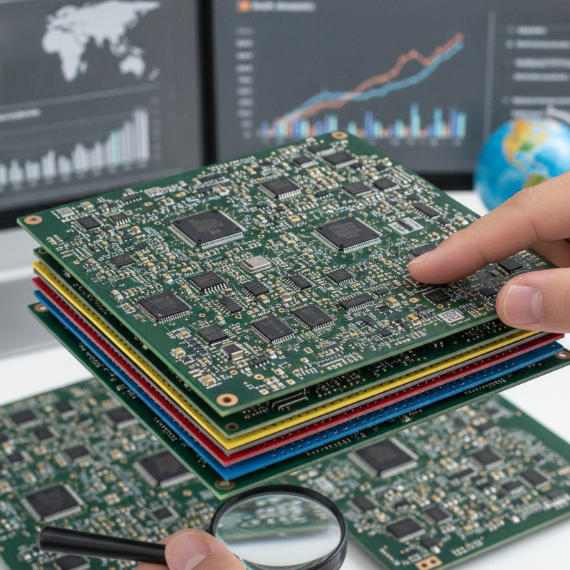
The Manufacturing Process of HDI PCBs
High-Density Interconnect (HDI) Printed Circuit Boards (PCBs) are crucial in modern electronic devices. The manufacturing process of HDI PCBs is complex and requires precision. These boards typically have higher than average wiring densities, leading to smaller, lighter products. The intricacies of the manufacturing process can directly influence performance and reliability.
The process starts with selecting high-quality materials. A typical HDI PCB is built using multiple layers. Manufacturers utilize advanced techniques such as microvia drilling, which creates very fine holes for electrical connections. A 2022 report by IPC stated that 40% of manufacturers have increased investments in HDI technology. This growth shows a strong demand for quality and efficiency.
However, the process isn’t without challenges. Achieving consistency in microvia placement remains a concern. Furthermore, issues like material quality variances can affect the manufacturing yield. The failure rates reported in various studies can reach up to 5% for certain production setups. Such statistics highlight the need for ongoing quality control and improvement. Collectively, these factors make mastering the HDI PCB manufacturing process essential for manufacturers aiming for global competitiveness.
What is HDI PCB and Why is it Essential for Global Buyers? - The Manufacturing Process of HDI PCBs
| Dimension | Value |
| Layer Count | 4-32 layers |
| Minimum Trace Width | 0.1 mm |
| Aspect Ratio | 1:12 |
| Surface Finish | HASL, ENIG, OSP |
| Applications | Smartphones, Tablets, Medical Devices |
| Manufacturing Time | 2-4 weeks |
| Quality Standards | IPC-A-600, IPC-6012 |
| Typical Materials | FR-4, Rogers, Aluminum |
Applications of HDI PCBs in Various Industries
HDI PCBs, or High-Density Interconnect Printed Circuit Boards, play a vital role across various industries. In consumer electronics, HDI PCBs are crucial. These boards allow for smaller devices with greater functionality. According to a market report, the HDI PCB market is expected to grow significantly, reaching approximately 20 billion USD by 2025.
In the automotive sector, HDI PCBs are essential for advanced driver-assistance systems (ADAS). These systems require compact, reliable boards that support multiple functions, from navigation to safety. Research indicates that about 35% of vehicles will incorporate ADAS technology by 2025, highlighting the need for HDI PCBs.
Tips: When selecting HDI PCBs, consider your product's environment. For instance, high temperatures can affect performance. Additionally, check throughput rates to avoid production delays.
In telecommunications, HDI PCBs enable 5G technology. The demand for faster data transfer requires intricate designs. Many manufacturers struggle with production consistency. Addressing these challenges is critical. With the right approach, HDI PCBs can enhance system performance while ensuring reliability.
Why HDI PCBs are Crucial for Global Buyers and Market Trends
High-Density Interconnect (HDI) PCBs are vital in modern electronics. They enable compact designs and enhanced performance. According to a recent industry report, the global HDI PCB market is projected to reach $24 billion by 2026. This reflects a CAGR of 10.3% from 2021 to 2026. Such growth emphasizes the increasing reliance on HDI technology across various sectors.
Global buyers benefit from HDI PCBs due to their efficient use of space and improved signal integrity. In devices requiring high reliability, such as medical equipment and smartphones, HDI's fine-line routing is essential. The electronics sector's rapid evolution demands these advanced PCBs. A study found that 60% of high-end consumer electronics now use HDI technology. This trend indicates a shift towards miniaturization. However, not all manufacturers are equipped to handle HDI production. Challenges in achieving the desired precision and quality exist.
Market trends show an increasing demand for multi-layer HDI boards. They allow for better heat dissipation and higher functionality. Many buyers need to weigh costs against the benefits of HDI. While HDI PCBs present opportunities, navigating their complexities can be daunting. This duality highlights the importance of reliable partnerships in PCB sourcing.


